|
|
 |

|
|
|
|
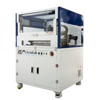
| SAM-DENEB |
| Scanning Acoustic Microscope for Semiconductor and Industrial Materials. |
|
|
|
 Kind Kind |
: |
SAM Products |
|

◎ Semiconductor : Flip Chip, BGA, QFT, TBGA, FBGA, SOP, FET, MLCC, PCB
◎ Industrial : ITO Target, Wafer, Pipe, Plate, Bar, complex Material, Piston test, Flaw detection in Planting, Car Engine, Weld zone

◎ The basic standard type SAM eqipment
◎ Measure the thickness of materials
◎ Measure the location and the size of flaw(Debonding, Delamination, Crack) inside materials and on the surface
◎ Low noise by using the highly efficient linear-servo motor
◎ High quality and accurate scanning image
◎ A, C, T Scan

| 1. Ultrasonic Pulser/Receiver |
| Frequency Range : 1 - 500MHz |
| Low noise, high performance pulser/receiver derives the ultrasonic signal of ultra wide-bandwidth characteristics from the transducer. |
| 2. A/D Converter |
| Real time 1GHz(8Bit) or 1.8GHz(12Bit) |
| 3. Mechanical Scanner |
| Scan Axis (Linear servo motor) |
Max. Stroke 350mm Max. Speed 1,000mm/s Repeatability +/-0.5 micron Encoder Resolution 0.5micron |
| Index Axis |
Micro-stepping motor with lead screw Max. Stroke 350mm Step Resolution 0.5micron |
| Vertical Axis |
Micro-stepping motor with lead screw Max. Stroke 70mm Vertical Resolution 2.5micron |
| 4. General |
| Water circulation pump with filter |
| Immersion Tank Dimension |
500mm x 520mm x 100mm |
| C- Scanning Area with T-Scan |
C-Scan 350mm X 350mm X 80mm
T-Scan 350mm X 130mm X 80mm |
| Main Unit SIZE |
970mm X 900mm X 1350mm |
| Weight |
Approx. 350kg |
| Power |
AC220V / 20A |
|
|
|
|
|